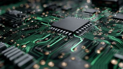
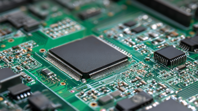
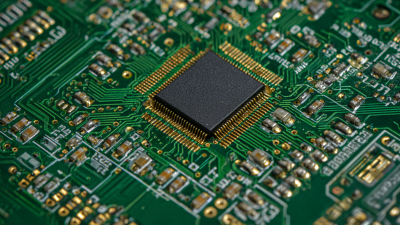
What is a Printed Circuit Board and How Does it Work?
Printed Circuit Boards (PCBs) are crucial in modern electronics. The global PCB market was valued at $60 billion in 2022, with expected growth to $80 billion by 2028, according to industry reports. As technology advances, the demand for efficient and reliable PCBs increases. They are integral in diverse sectors, from consumer electronics to aerospace.
Dr. James Liu, a PCB industry expert, states, "Every electronic device relies on printed circuit boards for functionality." This highlights their fundamental role. However, the industry faces challenges. Environmental concerns arise from PCB manufacturing processes. Recycling methods remain inadequate, and waste can be hazardous. Ensuring sustainability is a pressing issue.
PCBs need to adapt to evolving technologies. The rise of 5G and Internet of Things (IoT) demands thinner, more complex designs. Such innovations present opportunities and obstacles for manufacturers. Balancing quality and cost while addressing environmental impacts will shape the future of printed circuit boards. The journey ahead requires reflection and commitment from industry stakeholders.
What is a Printed Circuit Board (PCB)?
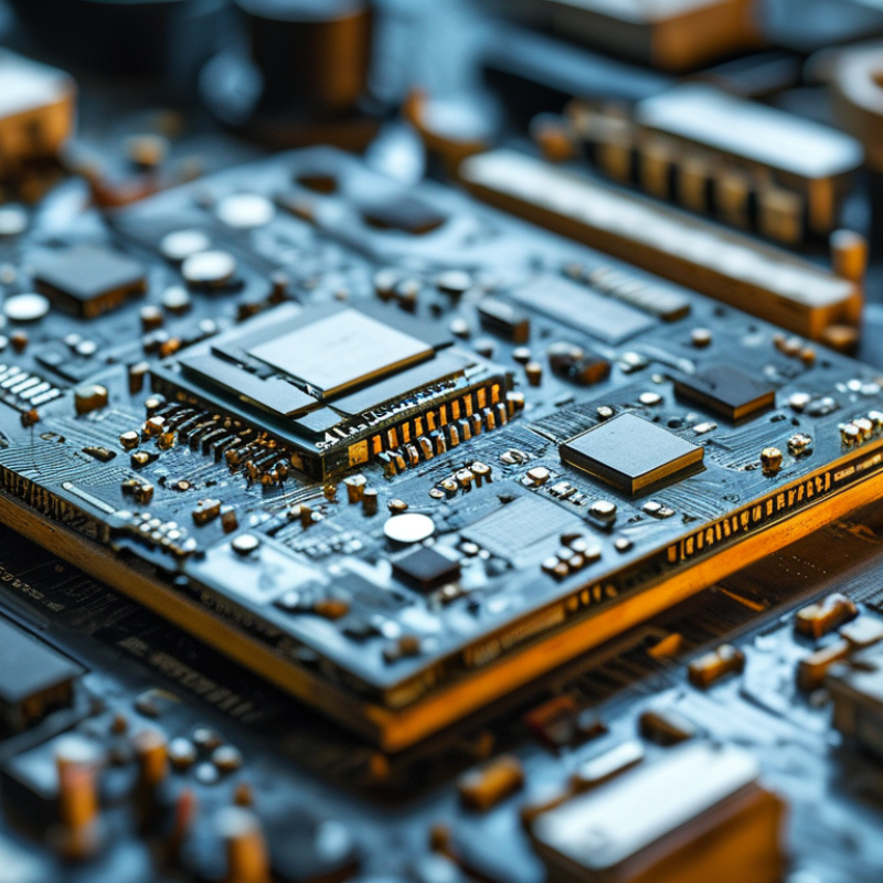
Printed Circuit Boards (PCBs) are essential components in modern electronics. They provide a foundation for electrical connections between various components. PCBs are made from insulating materials, such as fiberglass, with conductive pathways etched onto them. This technology enables complex circuits to be built compactly, which is crucial in devices like smartphones and computers.
According to a 2023 report by MarketsandMarkets, the global PCB market is projected to reach USD 90 billion by 2025. This growth reflects the increasing demand for consumer electronics and advanced automotive technologies. The trend towards miniaturization drives innovations in PCB design and manufacturing. Emerging technologies, such as flexible PCBs, offer new possibilities but also present challenges in durability and performance.
Despite their importance, PCBs are not without issues. Manufacturing defects can lead to failures in electronic devices. Additionally, environmental concerns arise from the disposal of PCBs containing harmful substances. The industry is actively seeking solutions, emphasizing the need for sustainable practices. As the demand for electronics continues to rise, addressing these challenges remains critical for the future of PCBs.
History and Evolution of Printed Circuit Boards
The history of printed circuit boards (PCBs) is fascinating and reflects the rapid progress in electronics. PCBs emerged during World War II. Engineers needed reliable and efficient ways to connect components. The advent of mass production changed everything. Before PCBs, wiring was labor-intensive and prone to errors. Early models used metal tracks on rigid boards. This innovation reduced assembly time and improved reliability.
In the 1950s, the technology evolved further. Multi-layer PCBs became possible, allowing for more complex circuits in a smaller space. This development was essential as electronics grew more sophisticated. PCBs began to enter consumer products, influencing a wide range of devices. However, challenges remained. The balance between size and functionality is never easy. Designers constantly faced limitations in materials and production techniques.
The evolution of PCBs also highlighted environmental concerns. As demand grew, so did the waste and pollution from production. The industry is now exploring eco-friendly materials. Despite these advances, some aspects of PCB design can still be improved. As technology changes, new solutions will emerge. The journey of printed circuit boards is an ongoing story, full of challenges and opportunities.
Components and Materials Used in PCB Design
Printed Circuit Boards (PCBs) are vital in today’s electronics. The components and materials used in PCB design determine performance and reliability. Common materials include FR-4, a fiberglass-reinforced epoxy resin. It creates a stable base and is widely adopted for its excellent dielectric properties. Industry reports suggest that FR-4 constitutes over 70% of the PCB market due to its balance of cost and performance.
Copper layers form the conductive pathways on PCBs. Most PCBs have a copper weight ranging from 1 to 3 ounces per square foot. Thicker copper layers enhance current-carrying capacity. Signal integrity and heat dissipation are also critical factors. However, with increasing circuit density, challenges arise, such as signal interference and heat management.
In addition to FR-4 and copper, other materials like polyimide are important for flexible PCBs. They offer resilience and are used in devices needing bending. The increasing demand for miniaturized electronics has driven interest in advanced materials. Yet, the increasing complexity of materials can lead to unforeseen issues during manufacturing. Such challenges prompt ongoing research in PCB technology.
How Printed Circuit Boards Function Electrically
Printed Circuit Boards (PCBs) are essential components in modern electronic devices. They provide mechanical support and electrical connections for various components. A PCB consists of a non-conductive substrate material, typically fiberglass or epoxy resin, which supports a conductive pathway made of copper traces. This design allows for the accurate routing of electrical signals, enabling devices to function correctly.
Electrically, printed circuit boards exhibit a fascinating balance of conductivity and capacitance. Research from industry experts indicates that approximately 70% of electronic failures stem from PCB design issues. Proper routing of traces is critical to minimize interference and ensure reliability. Engineers must be cautious with trace widths and spacing. The dielectric material's quality also plays a significant role in signal integrity. This complexity requires careful design and simulation, highlighting the importance of thorough testing.
A notable challenge in PCB function is the thermal management of components. As devices become more compact, managing heat dissipation becomes crucial. Poor thermal design can lead to component failure or reduced lifespan. Data from a recent report highlights that improper thermal management can reduce device reliability by up to 40%. This reality pushes designers to integrate better practices, such as using thermal vias and heat sinks, into their designs.
What is a Printed Circuit Board and How Does it Work? - How Printed Circuit Boards Function Electrically
| Dimension |
Description |
| Material |
Typically made from fiberglass, composite epoxy, or other materials providing insulation and structural integrity. |
| Layers |
Can vary from single-layer to multi-layer designs, influencing complexity and functionality. |
| Conductors |
Copper is commonly used for conductive paths that connect various components. |
| Functions |
Provides mechanical support and electrical connections for components such as resistors, capacitors, and microchips. |
| Manufacturing Process |
Involves several steps including design, etching, drilling, and soldering to create the final product. |
| Applications |
Used widely in electronics, telecommunications, military devices, and consumer appliances. |
Common Applications of Printed Circuit Boards in Modern Technology
Printed Circuit Boards (PCBs) are integral to countless modern technologies. In consumer electronics, PCBs enable the compact design of devices like smartphones and tablets. According to industry reports, the global PCB market is projected to reach $82 billion by 2026. This growth is driven by the demand for smaller, more efficient devices.
In the automotive sector, PCBs play a critical role in controlling various systems. Advanced Driver Assistance Systems (ADAS) depend heavily on reliable PCBs. A study indicated that the automotive PCB segment is expected to grow at a CAGR of 5.6% over the next five years. These boards are essential for functionalities like navigation, safety, and engine management. However, the increasing complexity of these systems can lead to design challenges.
Medical technology also showcases the versatility of PCBs. Devices like MRI machines and portable monitors rely on sophisticated PCB designs for precise functionality. The global market for medical PCBs is expanding, expected to exceed $4 billion by 2025. Yet, manufacturers face hurdles such as adhering to strict regulatory standards and ensuring reliability in critical applications. These challenges serve as a reminder of the continuous need for innovation in PCB design.