
What Is a PCB Board and How Does It Work?

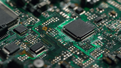
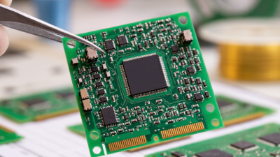
A pcb board is the physical foundation of many electronic devices, from a wireless mouse to a household router. It supports components and connects them through carefully patterned copper traces. At first glance, it may look like a flat green sheet. Look closer, and tiny pads, drilled holes, and narrow tracks reveal a compact electrical map. Small board. Big job.

When power enters a circuit, copper paths guide current between components. Signals travel along other traces, carrying information between chips, connectors, and sensors. Insulating layers keep conductive paths separated, while plated vias connect selected layers in multilayer designs. A resistor soldered near a processor may regulate current; a connector at the board’s edge links the device to the outside world. The layout matters. Trace width, spacing, and placement can affect heat, noise, and signal quality, so a pcb board is not merely a holder for parts.

Signal-integrity engineer and educator Eric Bogatin emphasizes that interconnects belong to the circuit itself. In paraphrase: “A trace is part of the circuit, not merely a connection.” That principle helps explain why board design requires more than drawing convenient lines. Designers consider materials, component locations, manufacturing limits, and how signals behave in real conditions. Still, a short introduction cannot capture every trade-off. Even a tidy board can behave unexpectedly when its materials, layout, or operating environment change. Understanding how its layers and paths work is a useful starting point—and a reason to examine the details carefully.
What Is a PCB Board and How Does It Work?

What Is a PCB Board?

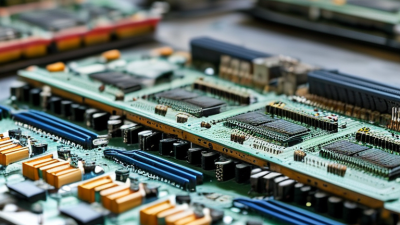
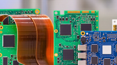
A printed circuit board (PCB) is a flat structure that holds electronic parts and connects them electrically. Despite the phrase “PCB board,” PCB already means printed circuit board. Most boards use an insulating base, often fiberglass-reinforced material, with thin copper layers. The copper is patterned into traces, pads, and planes. These paths carry signals and power between components. A board may have one layer or many, depending on its circuit and size requirements. Soldered components can include tiny resistors, chips, and connectors.

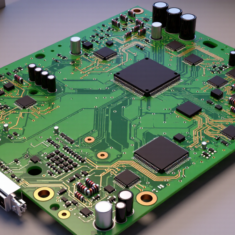
A PCB works like a carefully planned road map for electricity. A trace links two points, while the layout helps guide signals where designers intend. In multilayer boards, plated holes called vias connect copper layers. A protective solder mask covers most copper, leaving pads exposed for assembly. Small printed labels can identify parts and orientation. The board itself does not think; its components perform switching, sensing, or processing. That distinction is easy to miss. Narrow traces, heat, and vibration can affect reliability, so boards are inspected and tested before use.

Tips: When examining a PCB, look for copper traces, exposed solder pads, and component labels. A damaged trace may be difficult to spot, so visual inspection alone is not always enough.
What Materials and Layers Make Up a PCB?

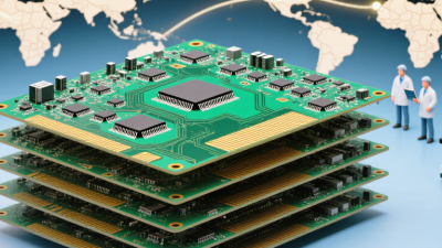
A PCB’s green surface hides a carefully bonded stack. Most rigid boards use FR-4, a laminate made from glass-fiber cloth and epoxy resin. Copper foil forms conductive traces on the outer faces and, in multilayer boards, inside the stack. Between copper layers, cured laminate cores and resin-rich prepreg provide insulation and mechanical support. On a two-layer board, the paths are easy to picture: one copper pattern on each side, joined by plated holes where needed.

Layer count changes the internal structure, not the basic recipe. A solder mask covers most copper, leaving pads exposed; silkscreen adds part labels and component outlines. IPC-4101 sets specifications for rigid printed-board base materials, including laminate and prepreg. The International Copper Study Group’s World Copper Factbook 2024 estimates global refined-copper usage at about 26.5 million tonnes in 2023. That figure covers all industries, not PCB production alone.

Tiny details matter. Trace spacing, resin choice, and glass weave can affect electrical performance and heat resistance. I would not treat FR-4 as a universal answer: fast signals or hot operating conditions may call for different laminates, and those choices can make fabrication less forgiving.

How Are Components Connected on a PCB?

On a PCB, components connect through copper pathways built into the board. A resistor or chip sits on small metal pads, and solder joins its contacts to those pads. The pads link to thin copper traces, which carry signals or power to other parts. Think of a trace as a narrow road under the green surface. It may look simple, but its width and route matter.

Some boards have several copper layers. A plated hole, called a via, connects a trace on one layer to another. This lets designers route connections beneath components or across the board without crossing every path on one surface. Power and ground often use wider copper areas, while delicate signals may need carefully controlled routes. The design is checked against a circuit diagram, since one misplaced connection can change how the whole device behaves. Small details count.

The explanation is tidy, perhaps too tidy. Real boards can include connectors, test points, and parts with many tiny contacts packed close together. A solder joint may look sound and still fail electrically, so inspection and testing matter. I used to think the copper did all the work; the solder joints are just as important.

How Does a PCB Work in an Electronic Device?

A PCB makes electrical connections between components while holding them in place. When a device receives power, copper traces carry current from the power input to parts such as a processor, sensor, or LED. A trace is not just a line on a drawing; its width and length affect resistance and signal behavior. Small design choices matter.

Consider a temperature sensor on a control board. It converts heat into a changing electrical signal. Copper traces route that signal to a processor, which interprets it and may switch on a fan. Ground paths help complete the circuit, while vias connect copper layers inside the board. In a multilayer PCB, some layers carry signals and others distribute power or ground. The path can be less tidy than a simple diagram suggests, especially when fast signals need careful routing. IPC’s 2022 World PCB Production Report estimated global PCB production value at about $81.5 billion, reflecting how widely these boards support electronic devices. That figure describes an industry, not how well any single board works; reliability still depends on its layout, materials, assembly, and testing.

What Is a PCB Board and How Does It Work? - How Does a PCB Work in an Electronic Device?

PCB Element What It Is How It Works in a Device Typical Example
Substrate The insulating base that gives a printed circuit board its shape and mechanical support. Supports components and separates conductive paths so they do not make unintended electrical contact. A rigid board commonly uses glass-reinforced epoxy laminate; flexible boards use bendable insulating materials.
Copper traces Patterned copper pathways on or inside the board. Carry electrical signals and power between components. Trace width and copper thickness affect current capacity and heating. A trace connects a sensor output to an input pin on a processing circuit.
Conductive layers One or more copper layers separated by insulating material. Provide routing space for connections. Multilayer boards can route signals on internal layers as well as outer surfaces. A four-layer board may use outer layers for signals and internal layers for power, ground, or additional signals.
Components Electronic parts mounted on the board, such as resistors, capacitors, diodes, and integrated circuits. Perform functions such as processing signals, storing charge, limiting current, switching, or regulating voltage. A resistor can limit current through an indicator light; an integrated circuit can process sensor data.
Pads and solder joints Exposed conductive areas and the solder that secures component leads or terminals. Create both a mechanical attachment and an electrical connection between a component and the board. Surface-mount component terminals are soldered to pads on the board surface.
Vias Plated holes that connect copper layers in a multilayer PCB. Allow electrical connections to pass between layers when a trace changes from one layer to another. A signal trace on the top layer can connect through a via to a trace on an internal layer.
Solder mask A protective coating applied over much of the copper surface, leaving selected pads exposed. Helps reduce accidental solder bridges and protects copper from handling and environmental exposure. The coating covers traces while component pads remain open for soldering.
Silkscreen markings Printed labels, symbols, and outlines on the board surface. Help identify components, polarity, connectors, and test points during assembly and servicing. A polarity mark can indicate the positive side of a polarized component.
Power and ground paths Conductive routes or planes that distribute supply voltage and provide a return path. Deliver electrical power to circuits and complete current paths back to the power source. A ground plane can provide a shared reference and a low-impedance return path when properly designed.
Signal path The route an electrical signal follows through components and copper connections. Carries information from an input, through processing or conditioning stages, to an output or another circuit. A sensor signal may pass through filtering circuitry before reaching a controller.

How Are PCBs Designed and Manufactured?

PCB design begins with a schematic: engineers connect components, then convert those connections into copper paths on a board layout. They choose the layer count, board thickness, trace widths, clearances, and materials. A high-speed signal may need a carefully controlled path between layers. Even a small change can affect impedance or fit.

Prismark’s 2022 global PCB industry forecast valued production at about $81.2 billion and projected $96.8 billion by 2027, roughly 3.6% annual growth. That scale makes manufacturability more than a factory concern. Designers check whether a fabricator can reliably drill each hole, register each copper layer, and solder the chosen components. The digital design is also reviewed for electrical and mechanical conflicts. Some early choices are hard to undo later.

Manufacturing turns the approved design into a physical board. Copper-clad laminate is imaged, etched, and laminated; multilayer boards are pressed together, drilled, and plated to connect their layers. Solder mask covers most copper, leaving pads exposed. Then the board receives labels, a surface finish, and electrical testing. Small errors matter. A board can look clean and still fail a continuity test, so test results and design files deserve a careful review before production.