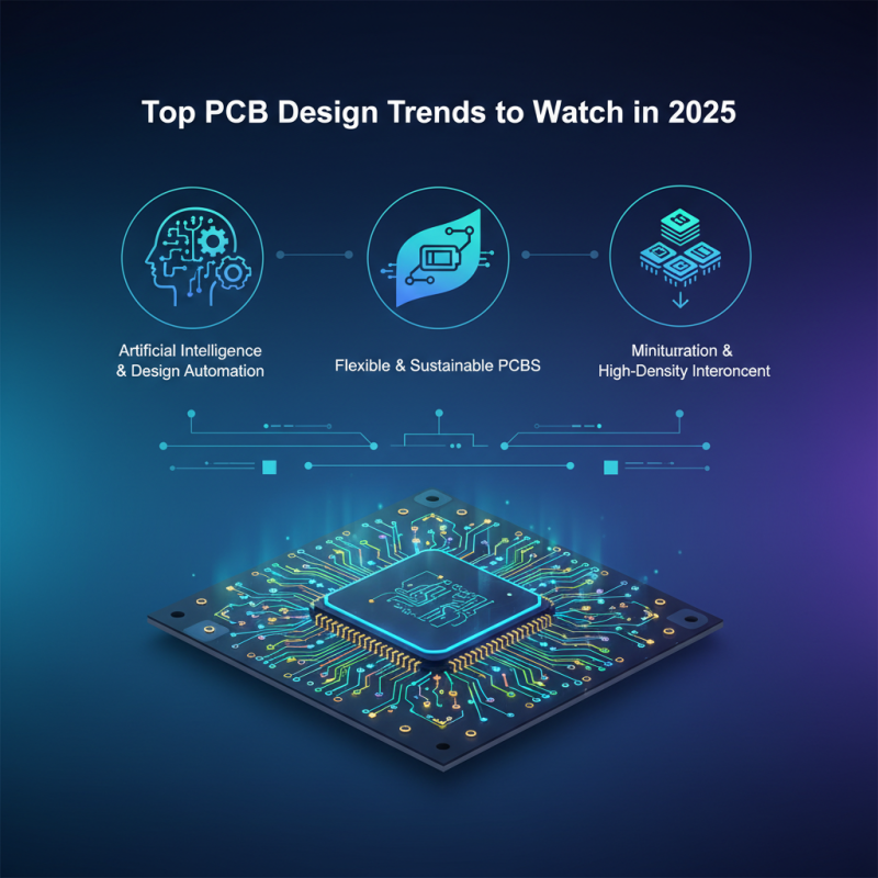
Top PCB Design Trends to Watch in 2025 for Innovative Electronics Development
As we look ahead to 2025, the landscape of electronic development is rapidly evolving, driven by innovative technologies and market demands. One of the key areas witnessing transformative changes is PCB design. With advancements in materials, manufacturing processes, and design software, engineers are pushing the boundaries of what’s possible in circuit board design. Emerging trends not only enhance performance but also cater to the growing needs for sustainability and miniaturization in electronic devices.
The future of PCB design is poised to incorporate cutting-edge technologies such as artificial intelligence, which will streamline design processes and improve accuracy. Additionally, the integration of flexible and printed circuit boards opens new avenues for creativity in device functionality and form factor. These trends, among others, reflect a broader shift towards smart, efficient, and adaptable electronics that can cater to diverse applications across industries.
As we explore the top PCB design trends of 2025, it becomes clear that the focus will be on enhancing efficiency, sustainability, and user experience. This not only signifies a paradigm shift in how electronic products are developed but also highlights the crucial role that PCB design will play in shaping the future of technology. Hence, staying attuned to these trends is essential for industry professionals aiming to remain at the forefront of innovation in electronics development.
Emerging Technologies Influencing PCB Design in 2025
As we approach 2025, the landscape of printed circuit board (PCB) design is being transformed by several emerging technologies. Notably, advancements in artificial intelligence (AI) and machine learning are enabling more efficient design processes, allowing engineers to automate repetitive tasks and optimize designs based on performance simulations. According to a recent industry report, AI in electronic design automation is projected to grow at a CAGR of over 30% from 2022 to 2026, highlighting its significant impact on PCB design workflows.
Furthermore, the rise of the Internet of Things (IoT) necessitates PCBs that can handle increased connectivity and data transfer rates. This demand for smarter, more connected devices is influencing design choices, pushing towards multi-layered boards that accommodate additional components and functionalities. The market for IoT PCBs is anticipated to exceed $100 billion by 2025, driven by innovations such as flexible PCB technologies and enhanced signal integrity features. As designers embrace these technologies, the focus on sustainability is also becoming paramount, with eco-friendly materials and processes gaining traction in PCB manufacturing.
These evolving trends in technology and design philosophy are set to redefine the PCB landscape, offering innovative solutions that meet the challenges of next-generation electronics development. With the confluence of AI, IoT, and sustainable practices, PCB designers are poised to lead the charge in creating smarter and more efficient electronic devices in the coming years.
Sustainable Materials and Eco-Friendly Practices in PCB Production
As the electronics industry continues to evolve, the emphasis on sustainability within PCB (Printed Circuit Board) production is becoming increasingly pronounced. A recent report by Allied Market Research projected that the global green electronics market is expected to reach $1 trillion by 2025, driven by consumer demand for eco-friendly products. This trend is influencing PCB manufacturers to adopt sustainable materials such as biodegradable resins and recycled substrates, which significantly reduce the environmental impact of electronics production.
In addition to using sustainable materials, eco-friendly practices are becoming integral to PCB manufacturing processes. According to a study conducted by IPC, over 70% of electronic manufacturers are implementing practices aimed at minimizing waste and energy consumption. The adoption of lead-free solder and the reduction of harmful chemicals in the production process have gained momentum, reflecting broader industry efforts to comply with environmental regulations and improve overall sustainability. As the industry moves towards a circular economy model, the integration of recycled materials is not just an option but a necessity for future PCB innovations.
Advancements in PCB Layout Techniques for High-Speed Applications
As we look ahead to 2025, advancements in PCB layout techniques are poised to play a critical role in the evolution of high-speed applications in electronics. With the increasing demand for faster data transmission and improved signal integrity, engineers are prioritizing designs that minimize electromagnetic interference (EMI) and optimize power distribution. According to a report by the IPC, a leading trade association for the electronic interconnection industry, over 50% of engineers now utilize advanced simulation tools during the design process to predict and mitigate potential issues before physical prototypes are manufactured.
Innovative techniques such as differential pair routing and controlled impedance designs are becoming mainstream as they facilitate the successful handling of higher frequencies. In particular, the rise of 5G technology and IoT applications has driven the need for designs that can support data rates exceeding 10 Gbps. A study from Research and Markets suggests that the global PCB industry is forecasted to reach a value of $75 billion by 2025, largely fueled by these high-speed demands. The adoption of multilayer boards and HDI (High-Density Interconnect) technology is also on the rise, enabling compact designs that enhance performance without compromising on reliability.
Additionally, the implementation of AI-driven design automation tools is revolutionizing PCB layout procedures. By leveraging machine learning algorithms, designers can innovate faster while reducing human error in complex layouts. As these technologies evolve, they will significantly impact how electronics are developed, pushing boundaries in high-speed applications, and ensuring that manufacturers stay competitive in an increasingly demanding market.
Top PCB Design Trends to Watch in 2025 for Innovative Electronics Development - Advancements in PCB Layout Techniques for High-Speed Applications
| Trend |
Description |
Impact on Design |
Expected Adoption Rate (%) |
| Flexible PCBs |
Adoption of flexible printed circuit boards to enable compact and lightweight designs. |
Allows for innovative form factors and improved reliability. |
75% |
| Embedded Components |
Integrating components directly into the PCB to save space and reduce assembly costs. |
Enhances thermal performance and simplifies assembly. |
65% |
| High-Frequency Materials |
Utilization of advanced materials for high-speed electrical performance. |
Improves signal integrity and reduces loss at high frequencies. |
80% |
| AI in Design Tools |
Incorporation of artificial intelligence in PCB design software. |
Increases design efficiency and optimization accuracy. |
70% |
| Thermal Management Techniques |
Advanced techniques to manage heat dissipation in high-performance PCBs. |
Enhances reliability and performance of electronic devices. |
60% |
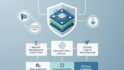
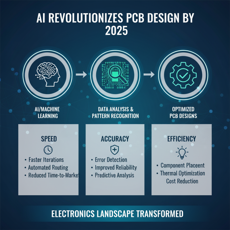
Integration of AI and Machine Learning in PCB Design Processes
The integration of artificial intelligence (AI) and machine learning in PCB design processes is anticipated to revolutionize the electronics landscape by 2025. As the complexity of electronic devices increases, traditional design methodologies often struggle to keep pace. AI-driven tools can analyze vast amounts of data from previous designs, identifying patterns and suggesting improvements that humans might overlook. This capability not only speeds up the design process but also enhances accuracy, leading to more reliable and efficient PCBs.
Moreover, machine learning algorithms can facilitate real-time simulations during the design phase. By predicting potential issues and suggesting design adjustments instantaneously, engineers can identify flaws earlier in the process, reducing prototyping costs and time. These intelligent systems can also optimize layout designs for performance and signal integrity, enabling the creation of smaller and more powerful devices. As industries strive for greater innovation, the synergy of AI and machine learning in PCB design will become a critical driver for new technologies and applications, advancing the field in ways previously thought impossible.
Trends in Miniaturization and Flexible PCB Development for Innovation
As we move toward 2025, the trends of miniaturization and flexible PCB (Printed Circuit Board) development are poised to significantly impact the innovative landscape of electronics. The global flexible PCB market is projected to grow at a CAGR of 14% between 2021 and 2026, reaching an estimated value of $36 billion by the end of this period, according to a recent market research report. This growth is driven by the increasing demand for lightweight and compact electronic devices, which have become essential in sectors such as consumer electronics, healthcare, and automotive industries.
The miniaturization trend is not only about reducing size but also enhancing functionality. Advanced manufacturing technologies like additive printing and laser etching enable the production of smaller, yet more efficient PCB designs. According to a report by IPC, the use of high-density interconnect (HDI) technology has surged, with over 40% of new PCB designs incorporating HDI features. This technology allows for more complex circuitry within a smaller footprint, making it a cornerstone of next-generation products that require high performance in constrained spaces. As designers increasingly focus on optimizing their layouts, the integration of flexible PCBs plays a critical role, allowing for innovative shapes and configurations that were previously unattainable in traditional rigid designs.
With the rise of wearable devices and IoT applications, the need for flexible and miniaturized PCBs will only increase. These advancements not only enhance performance but also open the door to new product designs that can adapt to various applications, further pushing the boundaries of what electronics can achieve.
Top PCB Design Trends to Watch in 2025
This chart illustrates the projected growth of various PCB design trends for 2025, focusing on miniaturization and flexible PCB development. The data highlights the increasing demand for these technologies in innovative electronics.