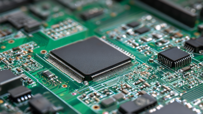
6 Effective Tips for Designing the Perfect Printed Circuit Board
The design of printed circuit boards (PCBs) plays a critical role in the performance and reliability of electronic devices, which have become ubiquitous in modern technology. According to a report from Research and Markets, the global PCB market is expected to reach $80 billion by 2025, driven by the increasing demand for consumer electronics and advancements in technologies such as 5G and IoT. As the complexity of electronic systems grows, so does the significance of effective PCB design, which can significantly influence manufacturing costs, time-to-market, and product functionality. Therefore, mastering the art of designing a perfect printed circuit board is essential for engineers and designers alike, ensuring that their products not only meet industry standards but also innovate in a highly competitive landscape. In this article, we will explore six effective tips for designing an optimal PCB that enhances both efficiency and performance.
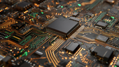
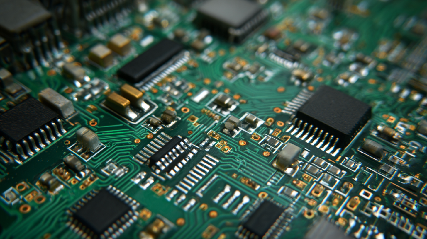
Understanding the Basics of Printed Circuit Board Design
Printed Circuit Boards (PCBs) are the backbone of modern electronic devices, serving as the foundational platform where components are assembled and connected. Understanding the basics of PCB design is crucial for engineers and designers aiming to create efficient, reliable circuits. According to a recent study from TechNavio, the global PCB market is projected to grow by approximately 4% annually from 2021 to 2026, highlighting the increasing demand for effective design methodologies.
One of the fundamental principles in PCB design is recognizing the importance of trace width and spacing, which directly affects the board’s electrical performance. The IPC-2221 standard provides guidelines for designing PCBs capable of handling specific current loads, emphasizing the need for meticulous calculations to prevent overheating and ensure durability. Additionally, leveraging specialized software tools can significantly enhance design accuracy, providing simulation capabilities that allow designers to foresee potential issues before production. As reported by P реагрti Pеn for Electronics Magazine, nearly 40% of PCB design time is spent on troubleshooting errors that could have been avoided with proper initial planning and design.
6 Effective Tips for Designing the Perfect Printed Circuit Board - Understanding the Basics of Printed Circuit Board Design
| Tip |
Description |
Important Considerations |
| 1. Define Specifications |
Clearly outline the requirements such as size, function, and performance. |
Understand power requirements and interfacing needs. |
| 2. Choose the Right Materials |
Select appropriate substrates and copper thickness for the PCB. |
Consider thermal and electrical properties of materials. |
| 3. Optimize Layout |
Arrange components for minimal trace lengths and optimal signal integrity. |
Plan for sufficient space between traces to avoid short circuits. |
| 4. Implement Proper Grounding |
Design a robust grounding plane to reduce noise and improve stability. |
Ensure all grounds are interconnected properly to avoid ground loops. |
| 5. Follow Design Guidelines |
Adhere to industry best practices and rules for PCB design. |
Use design software that checks for design rule violations. |
| 6. Prototype and Test |
Create prototypes to test and validate design before final production. |
Conduct thermal and electrical testing to ensure reliability. |
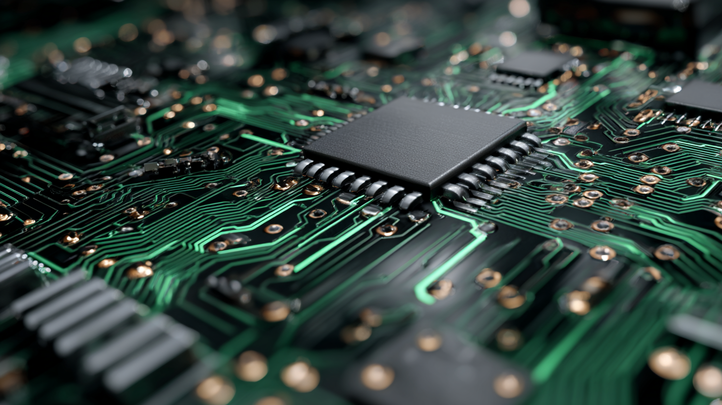
Choosing the Right Materials for Enhanced Performance
When designing the perfect printed circuit board (PCB), selecting the right materials is crucial for ensuring optimal performance and durability. The choice of substrate material impacts not only the electrical characteristics but also the thermal management of the PCB. Common substrates like FR-4, a fiberglass-reinforced epoxy laminate, offer a good balance of cost, mechanical stability, and electrical performance. However, for high-frequency applications, materials such as Rogers or Teflon might be preferable due to their lower dielectric constants and superior signal integrity.
In addition to the substrate, the choice of copper thickness and type can significantly affect the PCB’s overall performance. Thicker copper layers enhance current capacity and reduce resistive losses, making them ideal for power applications. On the other hand, thinner layers are suitable for high-density designs where space is limited. Moreover, incorporating advanced materials like polyimide can improve thermal resistance, which is essential for high-temperature environments. By carefully considering these material options, designers can enhance the reliability and efficiency of their printed circuit boards, ultimately leading to better functional outcomes in their electronic devices.
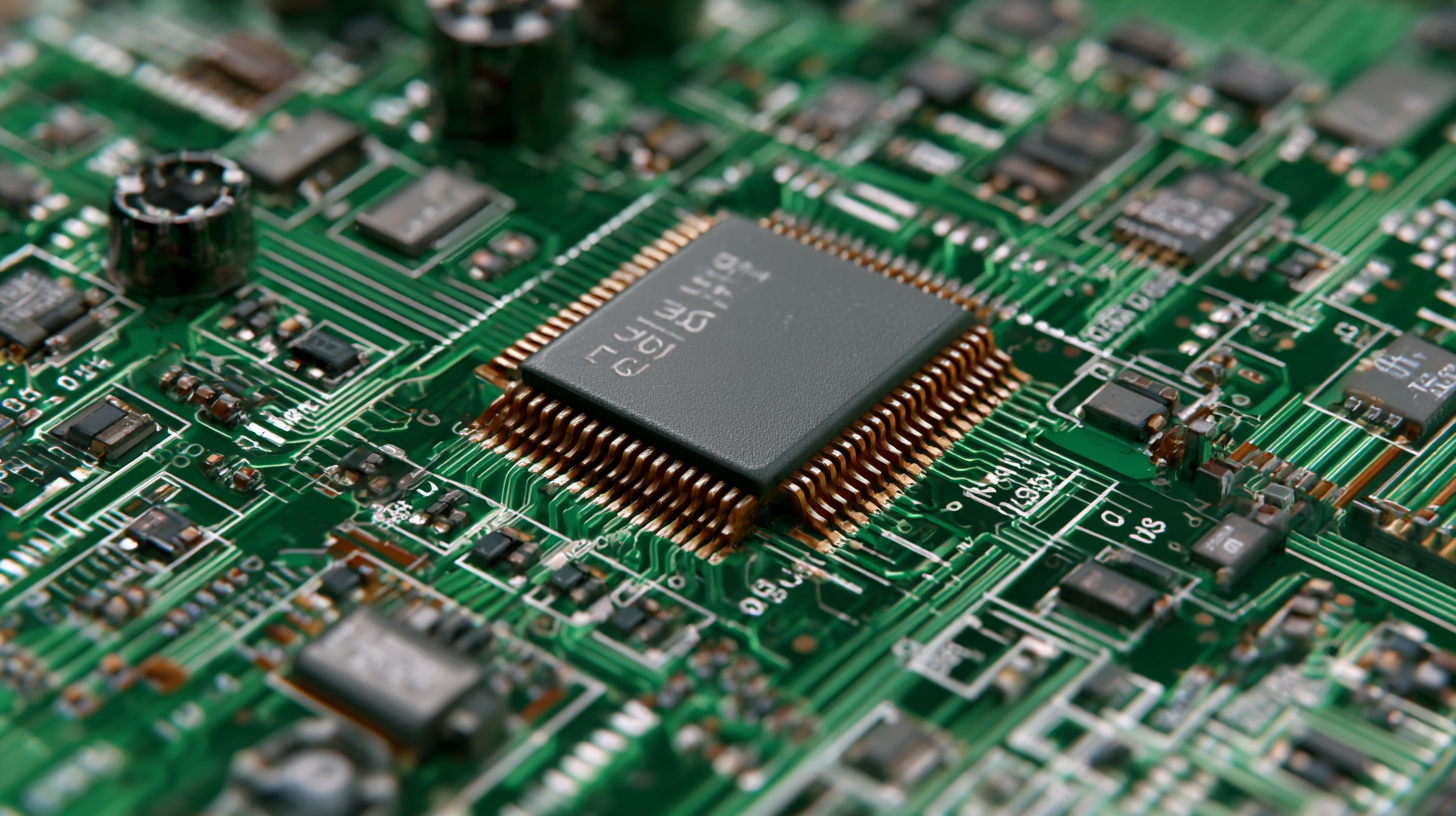
Implementing Effective Layout Techniques for Optimal Space Utilization
 Effective layout techniques are crucial in designing printed circuit boards (PCBs), especially when considering the importance of optimal space utilization. Just as sustainable building design emphasizes efficient space heating to reduce energy consumption, PCB design also seeks to minimize wasted space while maximizing performance. Employing strategies such as strategic component placement, efficient routing of traces, and effective layer stacking can enhance both functionality and manufacturability.
Moreover, adopting a holistic approach similar to the use of artificial intelligence in space design can lead to significant improvements. For instance, leveraging software tools that simulate thermal performance and signal integrity can optimize the PCB layout, ensuring that the board operates efficiently under varying conditions.
As organizations navigate the complexities of hybrid work environments, embracing flexibility in PCB design can also lead to innovative solutions that adapt to changing technological needs while conserving space and resources effectively.
Ensuring Signal Integrity with Proper Traces and Grounding
When designing printed circuit boards (PCBs), ensuring signal integrity is crucial, especially in high-frequency applications like wireless technologies. The quality of signal transmission is significantly influenced by factors such as trace length and the use of decoupling capacitors. In a CMOS inverter circuit, longer trace lengths can introduce unwanted inductance and capacitance, leading to signal degradation. A study by the IEEE found that reducing trace length by just 20% can improve the rise and fall times of the signal, ultimately enhancing the overall performance of the circuit.
To maintain optimal signal integrity, consider the following tips: First, employ a solid grounding strategy. A poor ground can result in ground bounce, which degrades signal quality—using a ground plane can help mitigate this issue. Second, place decoupling capacitors near power pins to filter high-frequency noise. Research indicates that strategically placed capacitors can reduce voltage fluctuations by nearly 50%, ensuring stable operation for sensitive components. Lastly, managing electromagnetic crosstalk through layout design—such as maintaining adequate spacing between traces and utilizing differential signaling—becomes increasingly important as devices shrink and operate at higher frequencies.
Adopting these practices can significantly enhance the reliability of PCBs, paving the way for innovative Bluetooth and Wi-Fi-enabled products that are both efficient and high-performing.
Testing and Iterating Designs to Achieve the Best Results
Testing and iterating designs are crucial steps in the development of printed circuit boards (PCBs) to ensure optimal performance and reliability. According to a recent report by IPC, approximately 51% of engineers identified design flaws as the most common reason for PCB failures. This underscores the importance of thorough testing protocols, such as functional testing and thermal analysis, to identify potential issues early in the design phase. By employing simulation tools and creating prototypes, engineers can refine their designs, which contributes to reducing time-to-market and overall costs.
In the pursuit of a well-designed PCB, it's beneficial to implement the following tips. First, prioritize a clear layout by organizing components effectively and minimizing trace lengths. A concise arrangement reduces signal interference and enhances performance. Secondly, incorporate design rule checks (DRCs) at every stage of development. These checks can spot common mistakes before they escalate into costly revisions later in the production cycle. Finally, gather feedback through iterative prototyping; real-world testing can illuminate weaknesses in the design that simulations may overlook. By embracing a cyclic process of prototyping, testing, and refining, engineers can achieve robust and efficient PCB designs that meet industry standards.