China Best PCB Board Design Tips and Techniques for Success?
In today's fast-paced electronics industry, effective PCB board design is crucial for success. A well-designed PCB can significantly enhance device performance and reliability. Yet, many designers grapple with common pitfalls in their PCB board design process.
Experience plays a key role in creating superior PCB designs. Understanding component placement and ensuring signal integrity are essential. However, even seasoned professionals can overlook these critical aspects. It’s vital to stay updated with new techniques and technologies that can improve design outcomes.
Attention to detail is a hallmark of successful PCB board design. Ensuring proper trace width, spacing, and ground connections can prevent costly errors. Learning from past mistakes is invaluable. Embracing challenges in design can lead to innovative solutions and improved project results. Balancing creativity and technical precision can be difficult but is necessary for impactful designs.

Essential Principles of PCB Board Design for Successful Projects
In the realm of PCB board design, a few essential principles stand out. Understanding the basics is crucial. Start with a clear schematic. This ensures all components are correctly represented and connected. Neglecting this step can lead to significant errors later. Precision is vital; even a tiny miscalculation can disrupt the entire project.
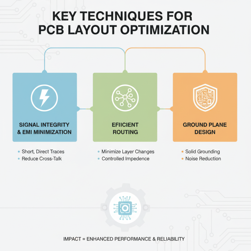
Layer management is another key principle. Properly organizing layers enhances signal integrity and reduces interference. Use ground planes strategically. They not only minimize noise but also improve thermal dissipation. However, be cautious. Overcomplicating layers can create confusion during assembly. Clarity is more beneficial than complexity.
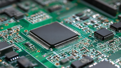
Don't overlook component placement. Positioning affects performance. Components that generate heat should be spaced apart. This reduces thermal buildup. Yet, the challenge lies in balancing space and accessibility. Striking this balance requires constant reflection and adjustment. Testing prototypes is essential. Feedback can reveal flaws overlooked during the design phase. Embrace these insights; they guide future improvements.
Best Practices for Selecting PCB Materials and Components
Choosing the right materials and components for your PCB is crucial for success. Start by assessing the specific requirements of your project. Factors like temperature, humidity, and electrical needs will guide your selection. High-frequency applications may require specialized substrates. These choices can significantly impact performance and durability.
Consider the environmental conditions your PCB will face. For example, if the board will be used in extreme temperatures, select materials that can withstand such conditions. Ensure your components are rated appropriately. A mismatch can lead to premature failure. Many designers overlook this aspect. It can be a costly mistake to address later.
Also, it's important to maintain a balance between quality and cost. While high-quality materials can improve reliability, they can also inflate production costs. Finding the right suppliers who offer a good compromise is essential. This requires research and sometimes testing various suppliers. Always document the performance of different materials in your projects for future reference. Aim for continuous improvement in your design practices.
Common Mistakes in PCB Design and How to Avoid Them
In PCB design, avoiding common mistakes is essential for success. A report from IPC indicates that a staggering 90% of design errors stem from inadequate planning. Insufficient understanding of design rules often leads to costly iterations. Designers must prioritize clear communication among team members. Poor documentation can create confusion and errors further down the line.
Overcrowded layouts pose another significant issue. An overly compact design can lead to signal integrity problems. It’s essential to allow proper spacing between components to avoid interference. A study by CADENCE shows that 60% of design failures arise from insufficient spacing, resulting in major performance issues. Regular audits and design reviews can help identify these pitfalls early in the process.
Thermal management is frequently overlooked as well. Many designers underestimate the heat generated by components. This oversight can lead to premature failures. Data indicates that 35% of PCBs fail due to thermal issues. Implementing proper thermal vias and heat sinks can mitigate this risk. Focusing on these common mistakes can greatly enhance the reliability and performance of PCB designs.